band gap diagram electric field
Semiconductor Devices Class 12 Part-1. 14 Pictures about Semiconductor Devices Class 12 Part-1 : Electric-Field Switching of Topological Phase, (a) Calculated electronic band structure of bilayer graphene on and also Delicately opening a band gap in graphene enables high-performance.
Semiconductor Devices Class 12 Part-1
 www.slideshare.net
semiconductor atomic
Delicately Opening A Band Gap In Graphene Enables High-performance
 phys.org
band graphene gap structure doped bilayer enables delicately al transistors si opening performance
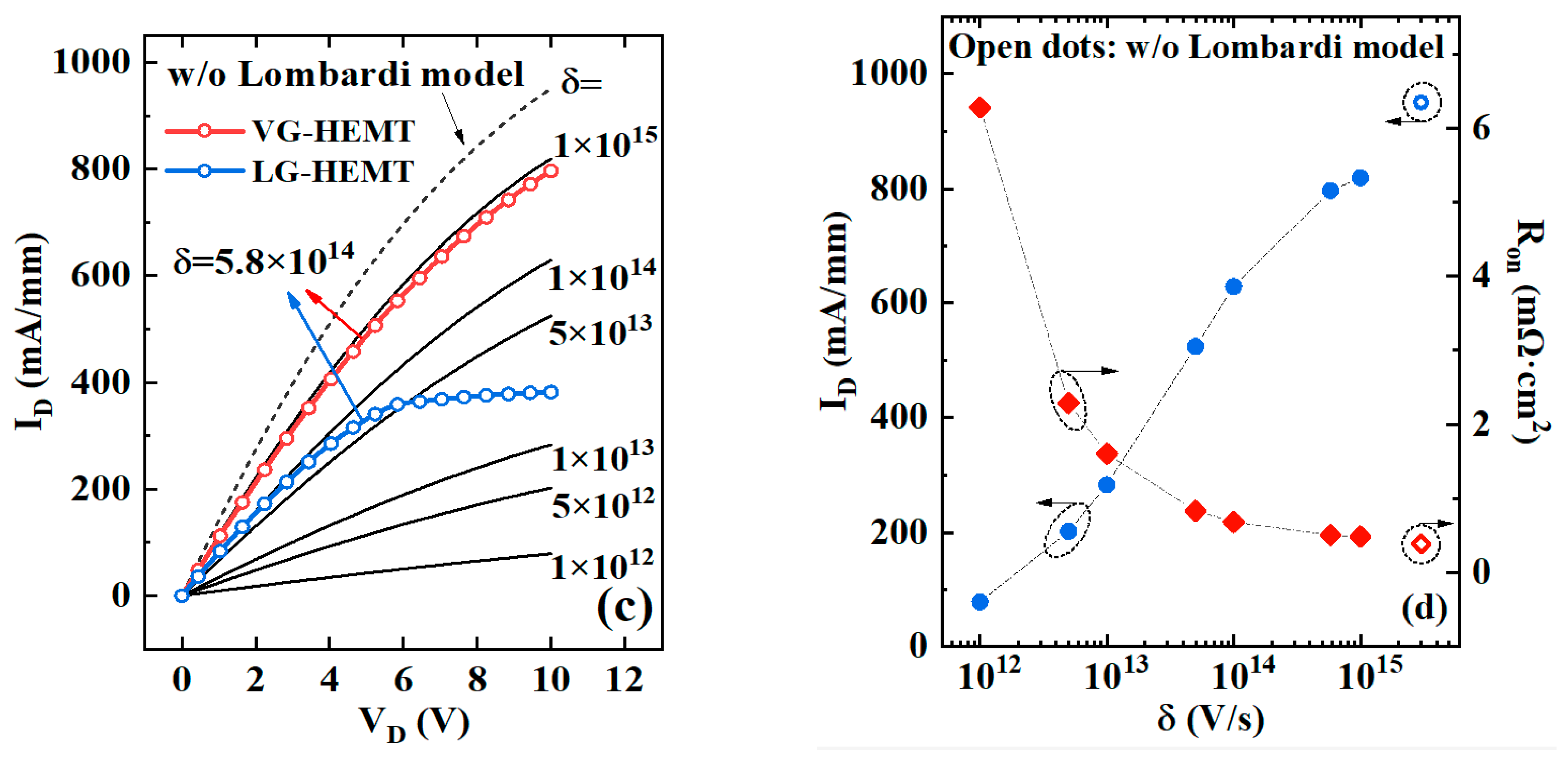
Answer: Energy Band Diagram And Electric Field For A Uniformly Doped N+
bipolar doped uniformly
The Calculated Energy Band Diagrams (a) And Electric Field
 www.researchgate.net
distributions al0 apd 17n 45n
Plot Of Band Gap Versus Lattice Constant Of Several | Download
 www.researchgate.net
lattice avalanche breakdown multiplication estimating inp photodiodes inalas
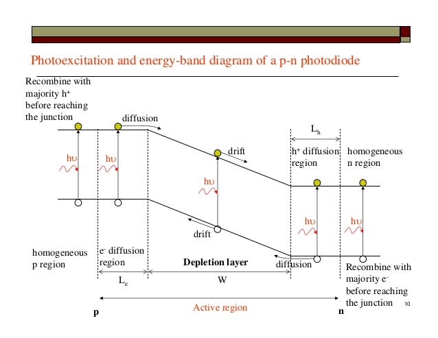
Lect12 Photodiode Detectors
 www.slideshare.net
photodiode detectors
Brevet US4471155 - Narrow Band Gap Photovoltaic Devices With Enhanced
 www.google.fr
brevets patent
(a) Calculated Electronic Band Structure Of Bilayer Graphene On
 www.researchgate.net
graphene bilayer electronic monolayer
Micromachines | Free Full-Text | A Novel GaN Metal-Insulator
 www.mdpi.com
micromachines gan
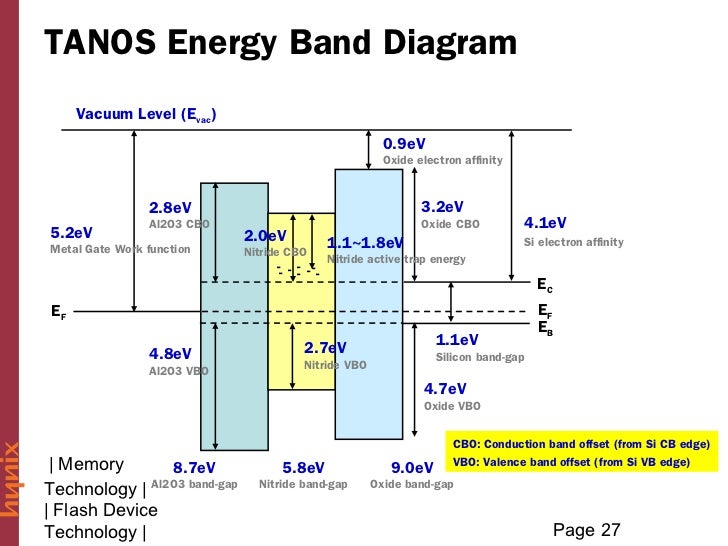
07.flash Memory Technology
 www.slideshare.net
conduction tanos cbo
Conduction In Solids
 www.rpi.edu
valence band electrons partially conduction filled bands energy electron conductor solids insulator fill animation diagram jump called states semi represents
Internal Band Gap Voltage Reference | Microchip
microchip
Semiconductor | Article About Semiconductor By The Free Dictionary
 encyclopedia2.thefreedictionary.com
semiconductor band gap diagram energy δε minima ge three figure width
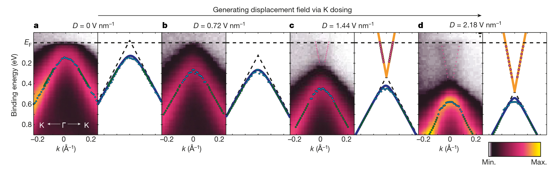
Electric-Field Switching Of Topological Phase
 als.lbl.gov
electric field switching topological phase structure band
Brevet us4471155. (a) calculated electronic band structure of bilayer graphene on. The calculated energy band diagrams (a) and electric field