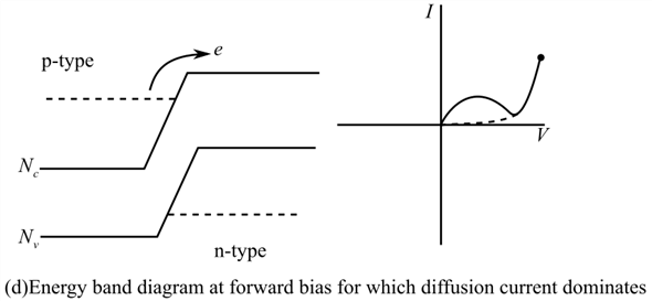
band diagram electric field
Electric field pattern on TE11 modes in a circular waveguide with. 17 Pics about Electric field pattern on TE11 modes in a circular waveguide with : pn junction - In band diagram, why the Fermi energy (EF) is constant, PN-Junction — Modern Lab Experiments documentation and also Electric field pattern on TE11 modes in a circular waveguide with.
Electric Field Pattern On TE11 Modes In A Circular Waveguide With
 www.researchgate.net
waveguide te11 modes polarization
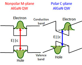
Enhanced Deep-UV Light Emission From Nonpolar M-planeAlGaN Quantum Wells
 www.brl.ntt.co.jp
quantum nonpolar algan plane band diagram wells enhanced emission uv deep light fig
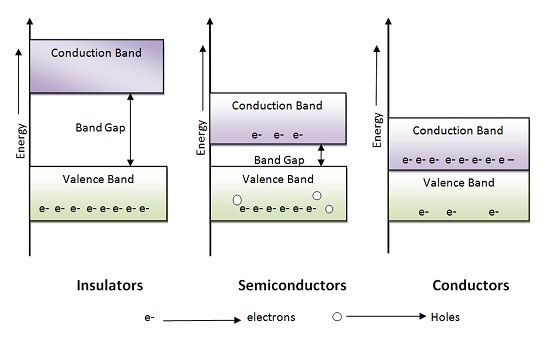
What Is Material? - Types, Semiconductor & Band Gap- Electronics Coach
 electronicscoach.com
semiconductor insulator conductor conduction electrons
Indirect-direct Band Gap Transition In BlueP/TMDs VdW Heterostructures
 www.researchgate.net
tmds vdw indirect heterostructures mos2 bluep wse2 ws2
Schematic Energy Band Diagrams For Edge And Bulk And 2-D ELT Diagram
 www.researchgate.net
diagram elt
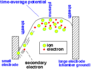
Capacitive Plasmas
 www.enigmatic-consulting.com
plasma sheath formation capacitive plasmas density field electric
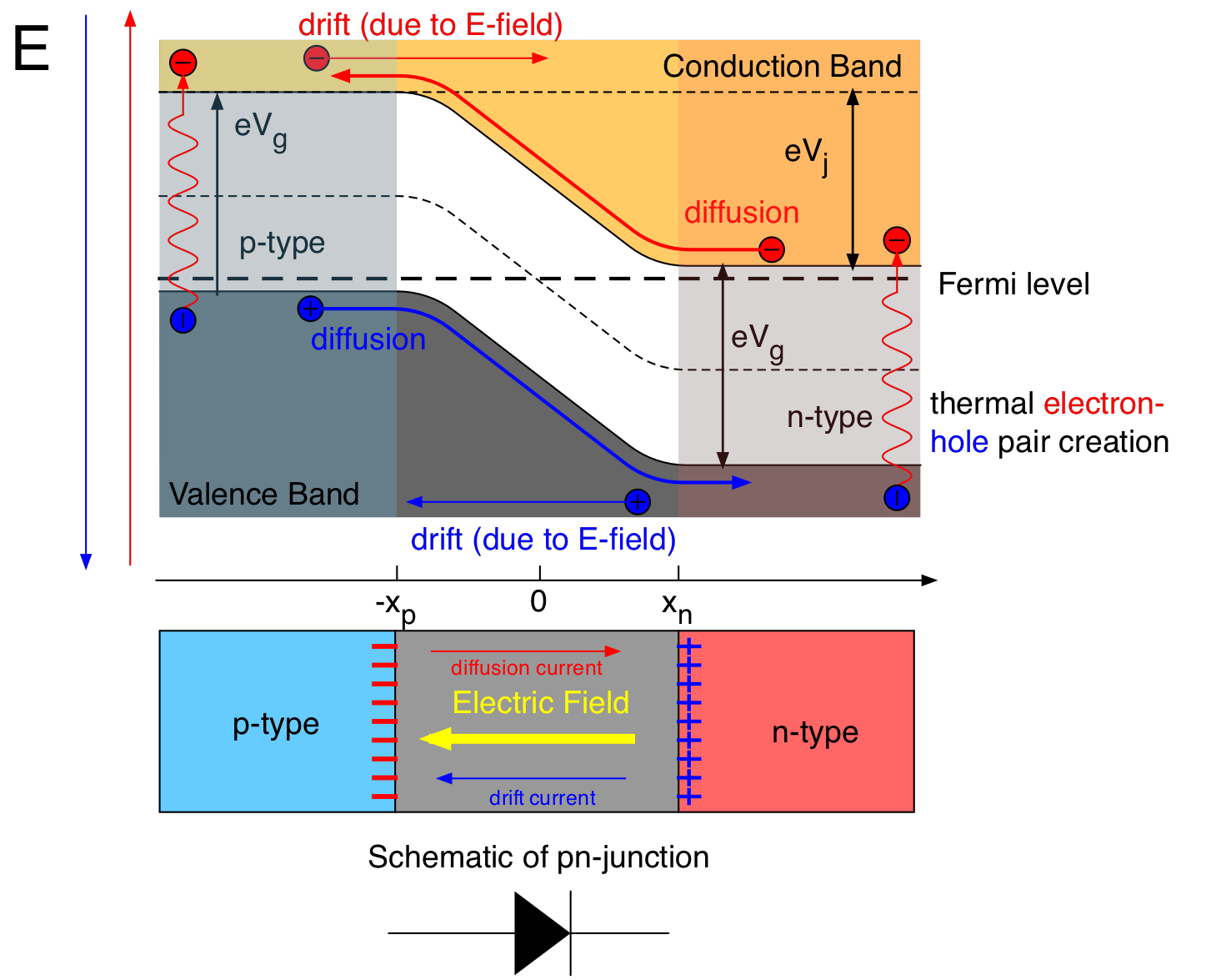
PN-Junction — Modern Lab Experiments Documentation
 wanda.fiu.edu
junction pn diagram energy silicon type state band electric semiconductor current quantum diode between location difference materials modern scheme field
Calculated Electronic Band Structures Under The Implemented External
 www.researchgate.net
implemented
Chapter 15 Solutions | Semiconductor Physics And Devices 4th Edition
 www.chegg.com
semiconductor physics
Detectors Of Light - Chemwiki
 chemwiki.ucdavis.edu
band semiconductor diagrams energy insulator conductor detectors light temperature chemwiki figure libretexts
Electric Field And Potential In A PN Junction | Band Bending
 www.youtube.com
junction field electric
Electric Fields And Conductors
 www.physicsclassroom.com
electric fields conductors field surface perpendicular stronger such
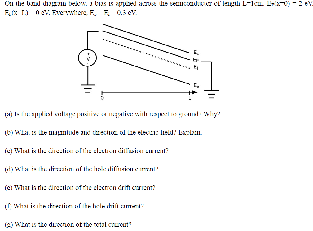
Solved: On The Band Diagram Below. A Bias Is Applied Acros... | Chegg.com
 www.chegg.com
semiconductor applied bias transcribed
Homework And Exercises - Electric Field Outside Wire With Stationary
 physics.stackexchange.com
wire field electric stationary outside current
Electric Field And Potential Distributions In Cable Without Cavities
 www.researchgate.net
potential cavities distributions
Pn Junction - In Band Diagram, Why The Fermi Energy (EF) Is Constant
 electronics.stackexchange.com
diagram band fermi energy ef pn device why junction level diagrams constant along source questions junctions stack
Energy Band Diagaram ( Conductor, Semiconductor And Insulator
 www.myelectrical2015.com
energy conductor band semiconductor diagram semi insulator revolution electrical flow
Electric field and potential distributions in cable without cavities. Enhanced deep-uv light emission from nonpolar m-planealgan quantum wells. Semiconductor applied bias transcribed